bonjour,
je me lance dans la fabrication d’un pcb v4.1,
après avoir fait les démarche sur le site de jlcpcb avec vérification et il pose quelques question avant de lancer la fabrication.
Hello,
Sorry to bother you, but there is an issue that we want to confirm with you before proceeding.
As shown below, you ordered 4 layer board, but there is no inner layers, only 2 copper layers, shall we make 2 layer board?
Sorry to bother you, but there are 2 thing that we want to confirm with you about your SMT order before proceeding.
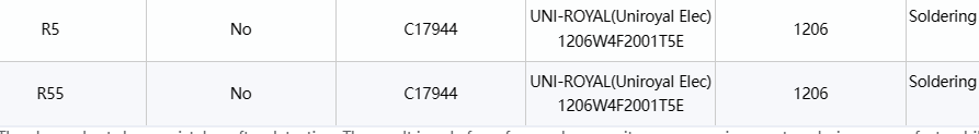
1 As shown below, seems the packages of the parts ( R5,R55) cannot match the corresponding pads on the PCB board, so we are unable to assemble them.
For this case there are 3 options for your choose as follows:
A- we enable the replace part button for you that you can re-select the corrected part
B- we leave this parts unpopulated and refund cost of the mismatch parts back to you to proceed and can’t ship the unsoldered parts with PCB due to the customs clearance issue,
C-cancel this PCB order and SMT order to place new order (there is no replace gerber file button for SMT order)
Pls consider and advise which case suits you, A or B or C??
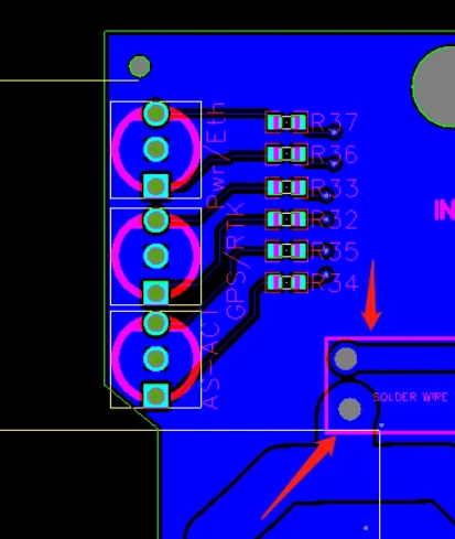
2As shown below, there’s no solder mask opening for below indicated pads in image 2. Here we have 2 suggestions.
A: Open them to be covered by tin. So that they can be soldered components.
B:Follow the file to cover them with solder mask ink.
La derniere version du std est 4.2, pas 4.1. Il faut aussi prendre le BOM dans le même dosier que le Gerber.
Pour les R5 et R55 tu as fait des subtitutions? ils devraient être de format 0603 pas 1206