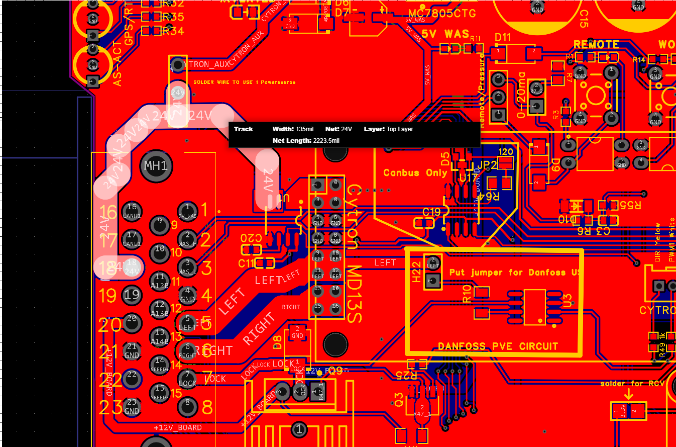
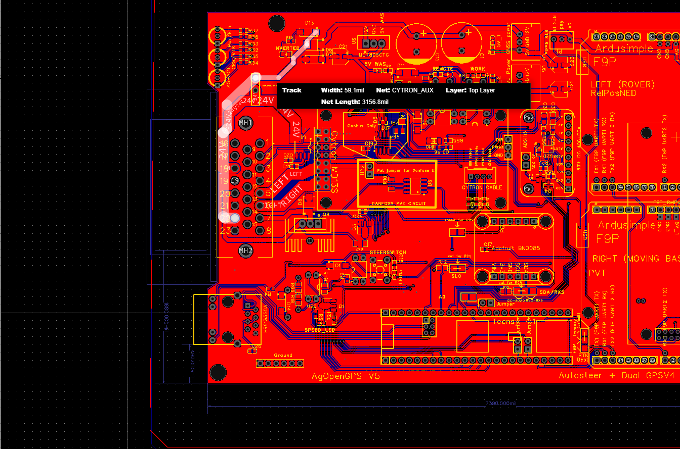
In my attempt to learn something new I ventured into the easyEDA world and made my attempt to modify the board so that the pin 18 and 22 were not connected only by a wire if wanting to use 12 v. pictures shows that I renamed the “net” name for the 24V trace to “24V” and moved some traces. The pictures show that the pin 18 and pin 22 traces are separate now. Does this look correct to the professionals on this forum as I am very much a novice at this? If this looks correct what steps do I take to put this into a Gerber file and possibly share with others on this forum. Just trying to contribute a little to this great project.
1 Like