Ok. Does rc11 have manual switches as well?
No it doesn’t.
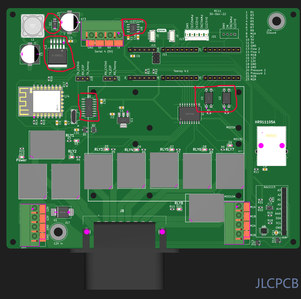
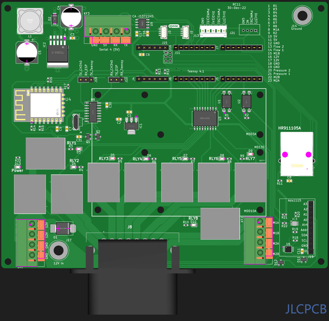
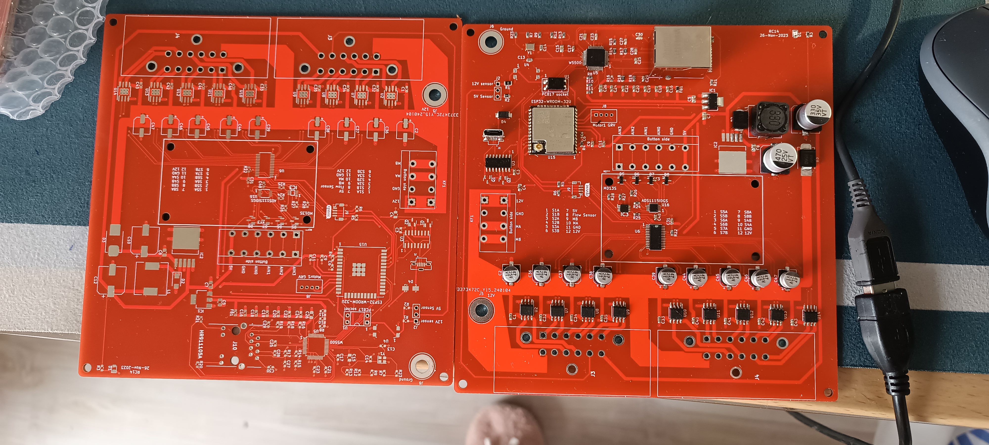
Can you please verfiy placement orientation is correct? The files uploaded to jlcpcb had some turned and I want to make sure I guessed correctly.
Thanks
Be careful, caps, diodes, ethernet plug also seem placed wrong, terribly wrong ![]()
Could you be more specific?
Yeah, I should have been specific.
I guess the picture from @SK21 is correct, I have not verified
The picture from @agriyields have many components in an other orientation, not only those he have circled.
I wonder why?
RC11:
I took files directly from GitHub to jlcpcb and that’s how the components oriented on the board. I was able to get them all correct I hope. Jlcpcb had D2 +- wrong way after I had it correct. So lots of verification, even after I sent image from GitHub of correct image.
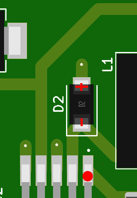
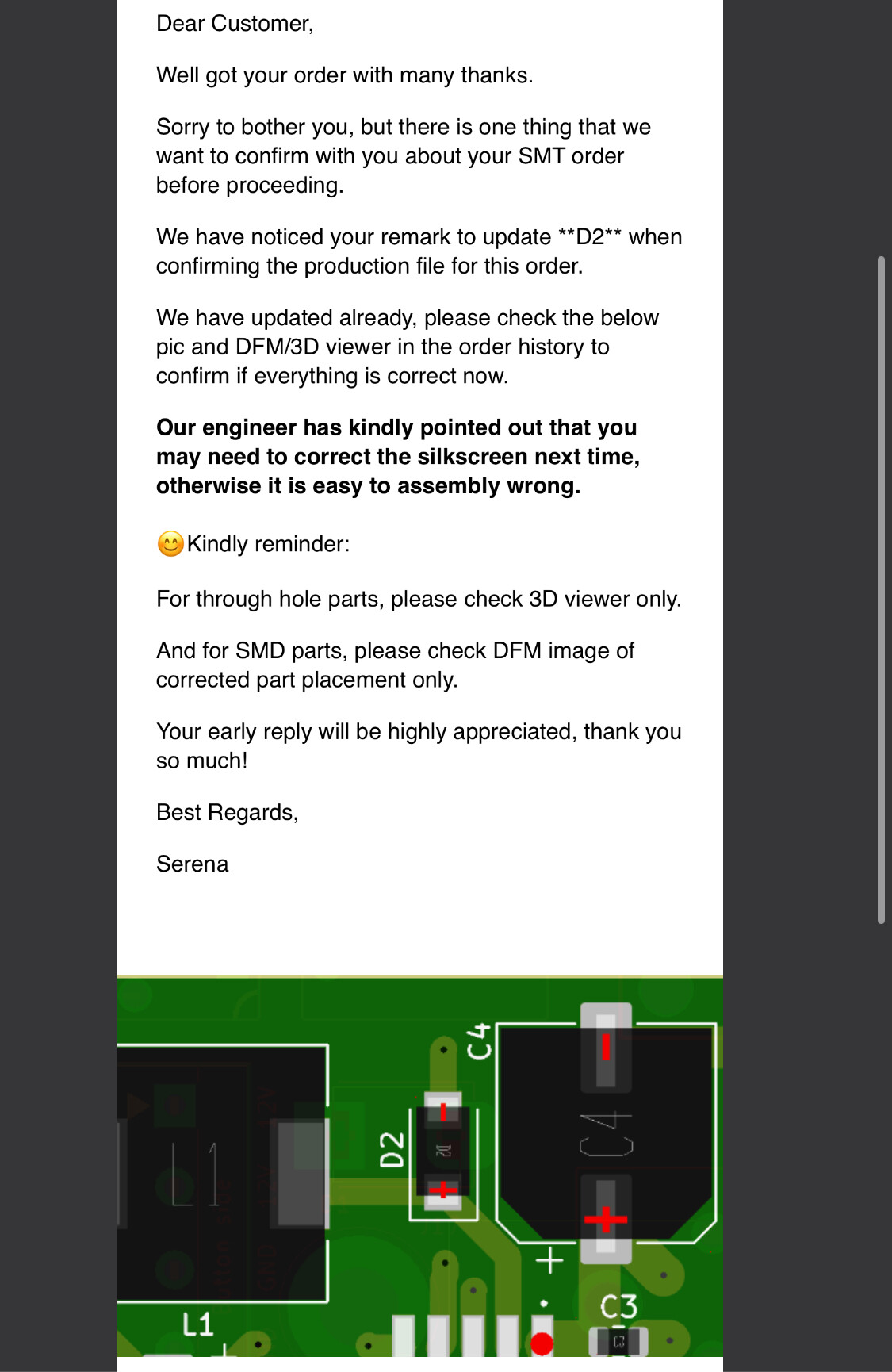
I don’t think that is correct.
But the cupper lines are not same in those two pictures, so not same board as both name D2.
But I would go with Serenas suggestion as it is supposed to be a zener diode and only allowing to connect to GND if voltage is higher than what that specific zener has in its specifications.
Edit: D2 seems to be a schottky flyback diode, not neccessaryly a zener as the symbol for D1 indicates.
Wiki mislead me as zener have several symbols. One is same as for a shottky .
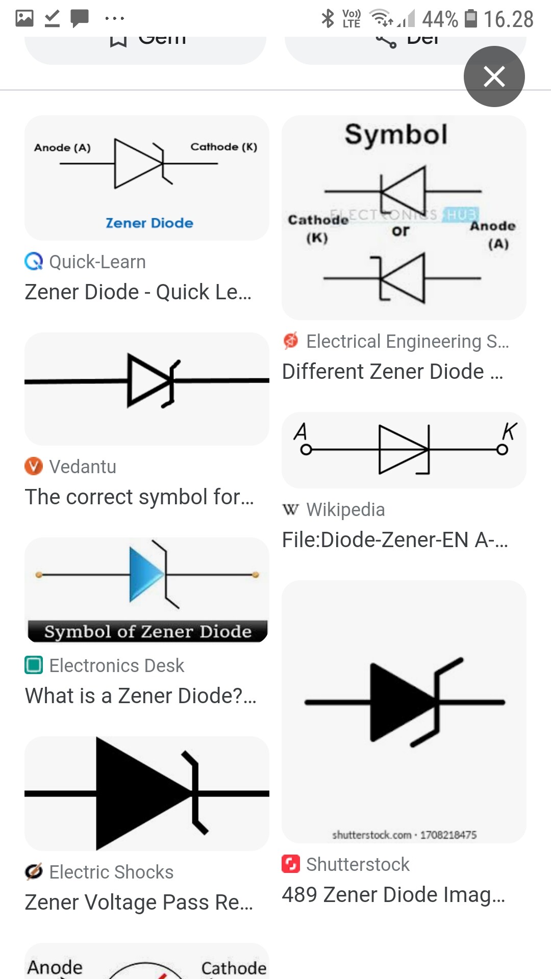
This is the diode:
I believe it is being used as a flyback diode. Maybe someone will more knowledge about this type of circuit could reply.
Apparently not me ![]() but yes D2 is probably flyback, as number of D1 in diagram is for a shottky diode, but symbol in same diagram is for zener diode
but yes D2 is probably flyback, as number of D1 in diagram is for a shottky diode, but symbol in same diagram is for zener diode
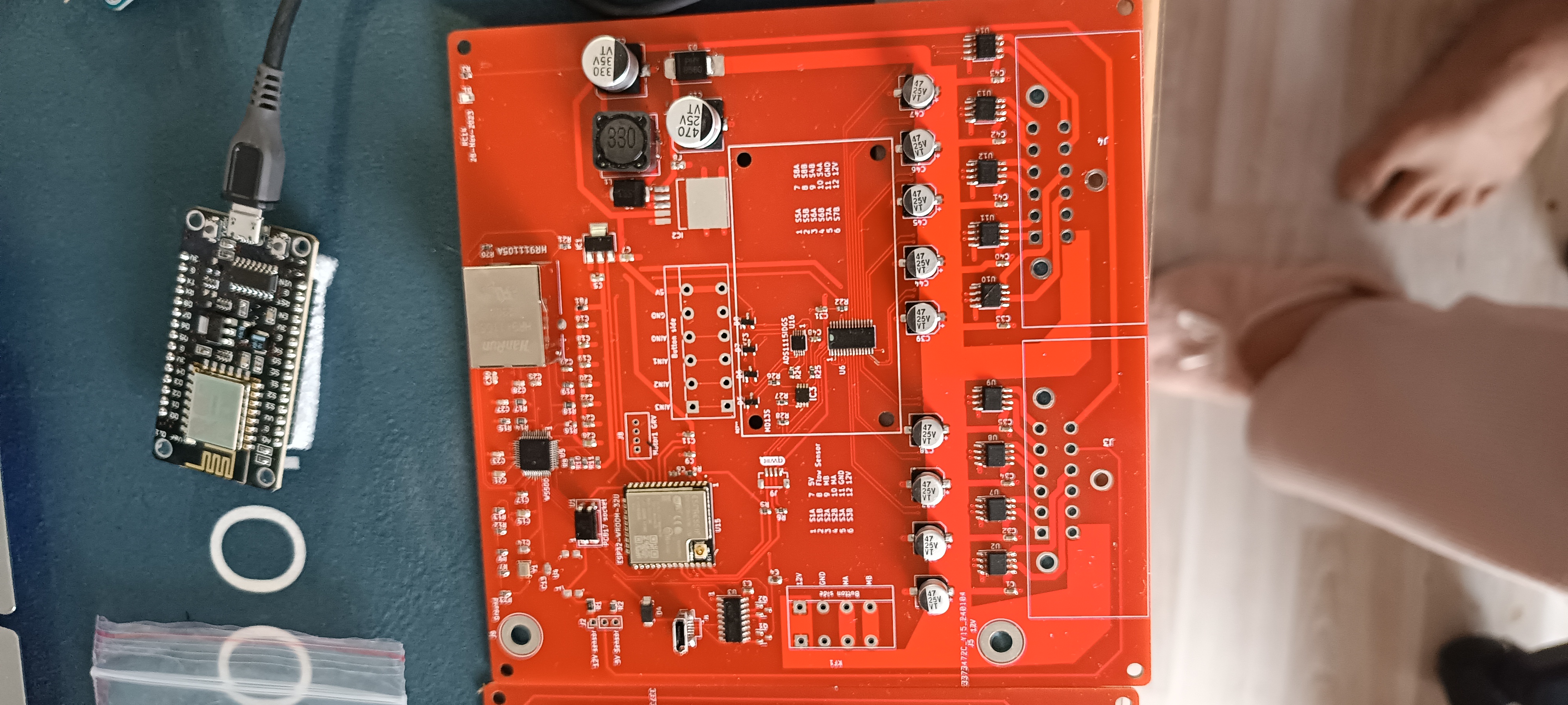
Using the one in GitHub as reference. If it’s not correct let me know, but I think others have posted it working.

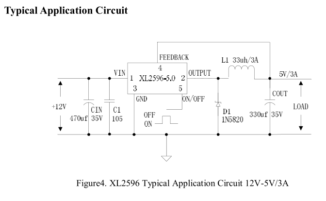
Most likely D1 here is a schottky diode and it’s correctly oriented according to the schematic. It’s there to prevent the OUTPUT/L1 connection from going below ground in-between OUTPUT pulses. This is needed due to the characteristics of inductors (L1).
I find the + - labels on the diodes and LEDs confusing, but I think the white polarity strip on the diode should be on the end of the diode connected to the trace between the chip and the inductor just like on the schematic. So when GND is more positive then the trace, the diode is supposed to conduct. I think that means the + should be on the GND side and - towards the trace.
This is correct. If it was the other way around the output of the xl2596 would go straight to ground.
I would like to buy complete ready to use PCB for my hardi sprayer. 7 sections. All stuff is arag stuff.
Anybody sell such things? I have agopengps in micro format so would be great to have PCB communications on ethernet or wifi
There are a few missing items left, the card is ready when the cargo arrives. Which code would you recommend?
1 Like
Hello. I collected the card, a few pieces are missing. Which code do you recommend I use?